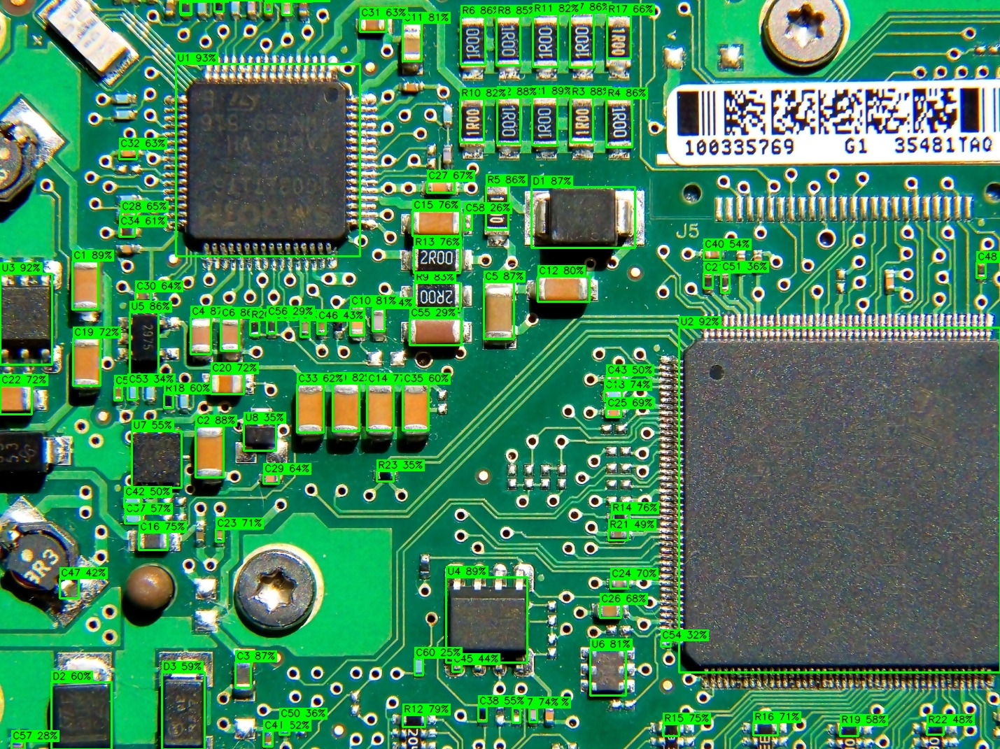
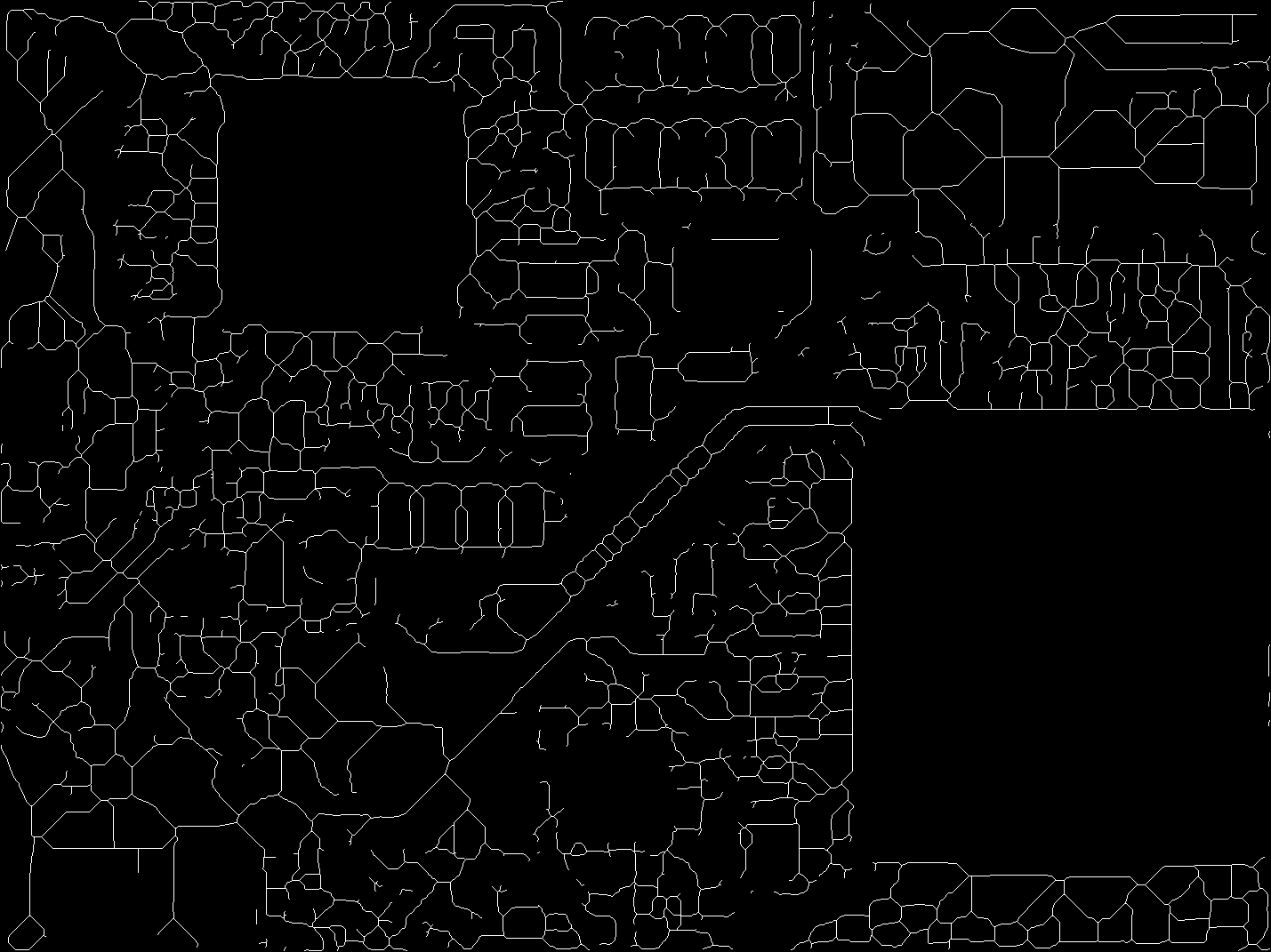
Our Goal: Reverse Engineer Every PCB in Minutes

Upload a photo of a circuit board. Get a complete schematic — components identified, netlist generated, ready to export.

BetaTraceAI is actively improving. Results may vary depending on board complexity, image quality, and component density. See full disclaimer →
Get Early Access (Beta)See How It Works →
TraceAI — PCB with AI component detection
Our Goal

Reverse engineering a PCB by hand takes days. It shouldn't.

No schematic, no BOM, no documentation. So you trace nets by hand and cross-reference datasheets for hours. TraceAI does it in minutes.

Three steps to a schematic.

01
Component detection.

Identifies resistors, caps, ICs, and connectors automatically from a single board photo. Accuracy improves with image quality and lighting.

02
Trace mapping.
Trace mapping.

Maps copper traces and infers connections between detected components. Results are best-effort and should be verified before use in production.

03
Export anywhere.
Export anywhere.

Export to KiCad, SPICE, or BOM. Fits the workflow you already use.

Built for hardware teams.

Legacy board repair

Recover schematics from discontinued products with no surviving documentation. Cut reverse engineering time from weeks to hours.

OEM manufacturing

Validate and document boards at production scale. Generate BOMs and schematics automatically as part of your QA pipeline.

Competitive teardowns

Understand how competing hardware is built. Identify key components and design decisions in minutes.

Education & research

Study real-world circuit design without expensive equipment or hours of manual tracing.

Get early access.

TraceAI is currently in beta. Join the waitlist for early access.

No credit card. No spam.